



Chemical Etched Copper Plate with High Precision Pattern
Category:
Key Words:
Product parameters
Parameter | Specification / Range |
Product Name | Etched Copper Sheet / Etched Copper Plate / Copper Component |
Material | Copper (C1100 / C1020) / Brass (optional) |
Thickness | 0.03 – 1.0 mm (customizable) |
Max Size | Up to 600 × 1500 mm (depending on material) |
Pattern Type | Micro holes / Slots / Complex etched patterns |
Minimum Feature Size | 0.03 – 0.10 mm (depending on thickness) |
Tolerance | ±0.005 – ±0.02 mm |
Edge Condition | Burr-free / Smooth edge |
Surface Treatment | Cleaning / Passivation / Polishing / Nickel plating / Tin plating |
Flatness | High precision control |
Manufacturing Process | Chemical Etching / Laser Cutting / Secondary Processing |
Conductivity | Excellent electrical conductivity (copper material) |
Structure Type | Flat sheet / Formed / Multi-layer |
Hole Type | Round / Square / Slot / Custom geometry |
Open Area | 10% – 70% (depending on design) |
OEM / ODM | Supported |
Drawing Format | PDF / CAD / DWG / DXF / STEP |
Sample | Available |
Lead Time | 5 – 15 days |
Packaging | Standard export packaging / Custom packaging |
Product Description
Product Description
Chemical etched copper plate featuring high precision patterns and excellent consistency. Compared with traditional stamping processes, chemical etching allows the creation of intricate geometries, fine features, and complex layouts without mechanical stress. This precision copper plate ensures smooth edges and stable performance in demanding applications.
Application Field
Ideal for precision components, electronic circuits, fine metal structures, and industrial parts. This etched copper plate is widely used in applications requiring high accuracy and repeatability.
Chemical Etched Copper Plate with High Precision Pattern
Our chemical etched copper plate offers a superior alternative to traditional manufacturing methods like stamping. This "non-contact" process allows for the creation of intricate geometries and fine features without inducing mechanical stress, ensuring smooth edges and stable performance in demanding applications.
At our factory, we utilize advanced photo-chemical machining to produce precision copper plates that meet the highest standards of accuracy. By digitally controlling the etching process, we can achieve complex patterns that are impossible or prohibitively expensive with hard tooling. This makes it the ideal choice for engineers requiring high repeatability and zero burrs.
The Science of Precision Etching
Chemical etching is a subtractive manufacturing process that uses corrosive chemicals to dissolve metal selectively. Unlike laser cutting, which uses heat, or stamping, which uses physical force, etching is a "cold" process. This means the material properties of the etched copper plate remain unchanged, with no heat-affected zones (HAZ) or micro-fractures.
Key Process Advantages
- Zero Mechanical Stress: Since no physical force is applied to the metal, the copper plate remains perfectly flat. This is critical for thin materials that would otherwise warp or deform under the pressure of a stamping die.
- Intricate Geometries: We can produce complex patterns, including fine meshes, grids, and conductive traces, with absolute consistency. The digital nature of the tooling means design changes are instant and cost-effective.
- Burr-Free Edges: The chemical dissolution process leaves edges smooth and clean. This eliminates the need for secondary deburring operations, saving you time and cost in assembly.
- Micro-Precision: Our advanced etching lines are capable of achieving a minimum aperture of 0.1mm. This micro-level capability allows us to manufacture ultra-fine filters, optical apertures, and precise electronic components.
Process Comparison: Etching vs. Traditional Methods
To help you select the best manufacturing method for your project, we have compared chemical etching with laser cutting and stamping.
Chemical Etching vs. Laser Cutting
While laser cutting is versatile, it faces challenges when processing highly reflective metals like copper.
- Heat Management: Laser cutting generates significant heat, creating a Heat Affected Zone (HAZ) that can alter the conductivity and structural integrity of the copper. Chemical etching generates no heat, preserving the material's original properties.
- Edge Quality: Lasers can leave burn marks or dross (slag) on the edges. Our chemical etched copper plate features clean, smooth edges right off the production line.
- Speed: For parts with thousands of holes (like fine meshes), etching is significantly faster as it removes material simultaneously rather than cutting sequentially.
Chemical Etching vs. Stamping
Stamping is a traditional method, but it lacks the flexibility required for modern precision engineering.
- Tooling Costs: Stamping requires expensive, hard steel dies that take weeks to manufacture. We use digital photo tools, which are inexpensive and can be ready in hours.
- Design Limitations: Stamping struggles with very thin or very hard materials due to the physical force required. Etching handles these materials with ease, offering greater design freedom for precision components.
Technical Specifications
Our production capabilities are designed to handle the most demanding specifications for industrial and electronic applications.
Parameter | Specification |
|---|---|
Process | Chemical Etching (Photo Chemical Machining) |
Material | Copper, Brass, Stainless Steel, Aluminum |
Min. Hole Size | 0.1mm (Micro Precision) |
Thickness Range | 0.03mm – 2.0mm |
Tolerance | ±0.01mm – ±0.05mm |
Surface Finish | Smooth, Burr-Free, No Recast Layer |
Applications of High-Precision Etched Plates
Our precision copper plates are widely used in industries where accuracy and reliability are non-negotiable.
- Electronic Circuits: Used for creating precise conductive pathways, shielding grids, and battery contacts where electrical resistance must be minimized.
- Precision Components: Ideal for encoder discs, optical apertures, and sensor parts that require exact dimensions and light transmission.
- Fine Metal Structures: Perfect for decorative meshes, speaker grilles, and filtration screens where aesthetic quality and structural integrity are key.
- Industrial Parts: Used in gaskets, shims, and lead frames that require flatness and consistent thickness.
Our Production & Quality Control
We understand that consistency is key in industrial manufacturing. Our factory employs a rigorous quality control process for every etched copper plate we produce.
- Digital Tooling Verification: We verify all Gerber files to ensure the photo tool matches your design exactly.
- Cleanroom Preparation: The metal surface is cleaned meticulously to ensure perfect adhesion of the photoresist.
- Etching Monitoring: Our automated lines monitor chemical concentration and temperature to ensure uniform etching rates across the entire sheet.
- Optical Inspection: Finished parts undergo optical inspection to verify dimensions, hole sizes, and surface quality against your specifications.
Discuss Your Complex Pattern with Our Engineers
Do you have a design that requires micro-precision or complex geometries? Our team is ready to evaluate your requirements and provide a solution that balances performance with cost-efficiency.
Contact us today to discuss your project specifications.
- WhatsApp: +86 12132219094
- Factory Location: Shenzhen, China
Questions and Answers
Frequently Asked Questions (FAQ)
Here are answers to common technical questions regarding our chemical etching services.
Q: What is the smallest hole size you can etch in copper?
A: We have achieved a minimum aperture of 0.1mm using our micro-etching technology. This allows us to produce highly detailed patterns for filtration and optical applications.
Q: Does chemical etching affect the conductivity of the copper?
A: No. Since chemical etching is a cold process without heat or physical deformation, the electrical and thermal conductivity of the copper remains exactly the same as the raw material.
Q: Can you etch half-etched areas (countersinks)?
A: Yes. One of the unique advantages of our process is the ability to etch to different depths on the same sheet. We can create "half-etched" lines or folds, which allows the metal to be bent into 3D shapes without cracking.
Q: How does the cost compare to laser cutting for mass production?
A: For complex parts with many features (like meshes or grids), chemical etching is often more cost-effective than laser cutting for medium to high volumes because it processes the entire part simultaneously, significantly reducing machine time.
Q: What file formats do you accept for tooling?
A: We primarily work with vector-based files such as DXF, DWG, or Gerber files. This ensures that the intricate geometries of your precision copper plate are translated perfectly into the photo tool.
Factory Description
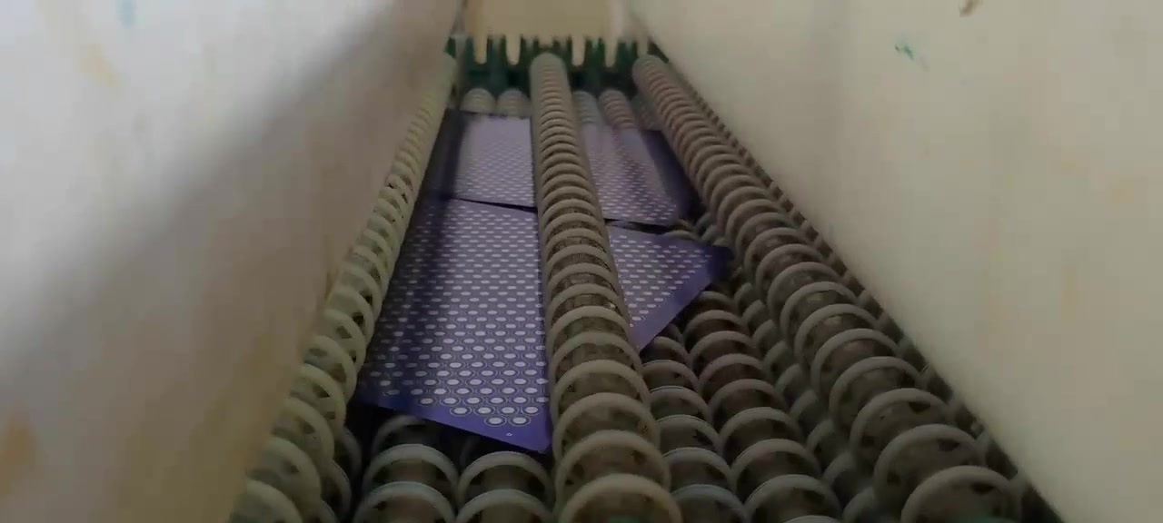
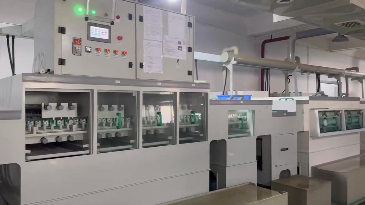
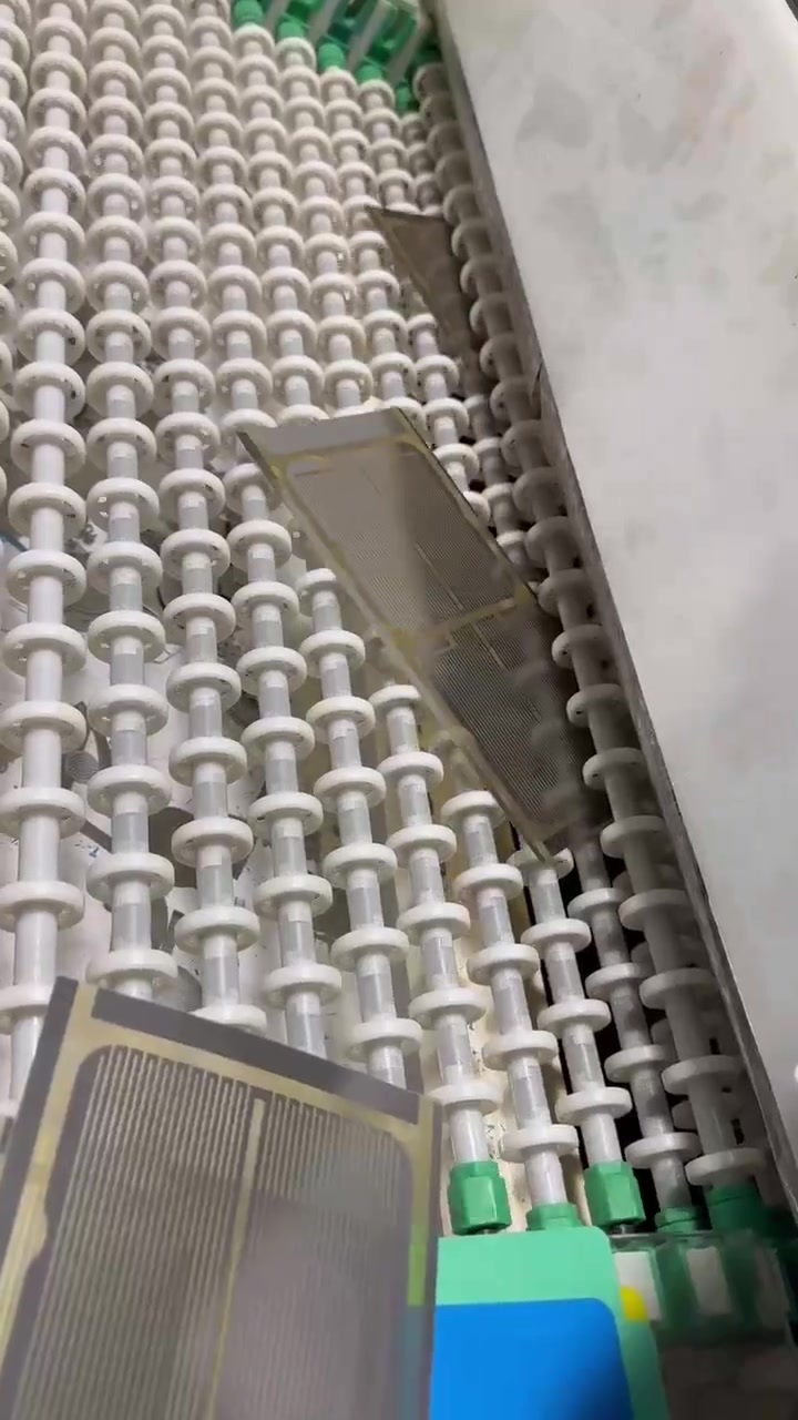
We have a full set of etching production equipment and mature processing technology. We can manufacture products in any shape with mesh sizes as small as 0.1mm, according to your requirements.

Our Advantage
Factory Direct Shipping
Our products undergo 100% QC checks before shipment, and we ensure compliance with international standards. If you require specific certifications for your target market, just let us know, and we'll meet those requirements.
Experienced Design and Manufacturing Team
We work closely with customers from the design phase to help avoid potential product flaws, ensuring both the functionality and design meet expectations.
Excellent Supply Chain Management
We can quickly adjust production schedules to meet your urgent deadlines, whether it's for large bulk orders or smaller rush orders.
OEM & ODM Support
We offer the option to print your logo or other customizations.
Strict Quality Control
Our products undergo 100% QC checks before shipment, and we ensure compliance with international standards. If you require specific certifications for your target market, just let us know, and we'll meet those requirements.
Certificate
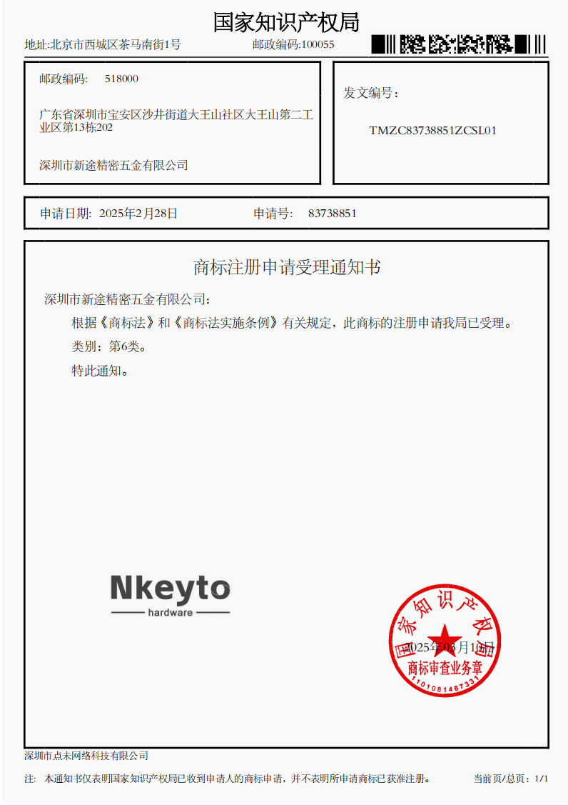
商标6类

9001
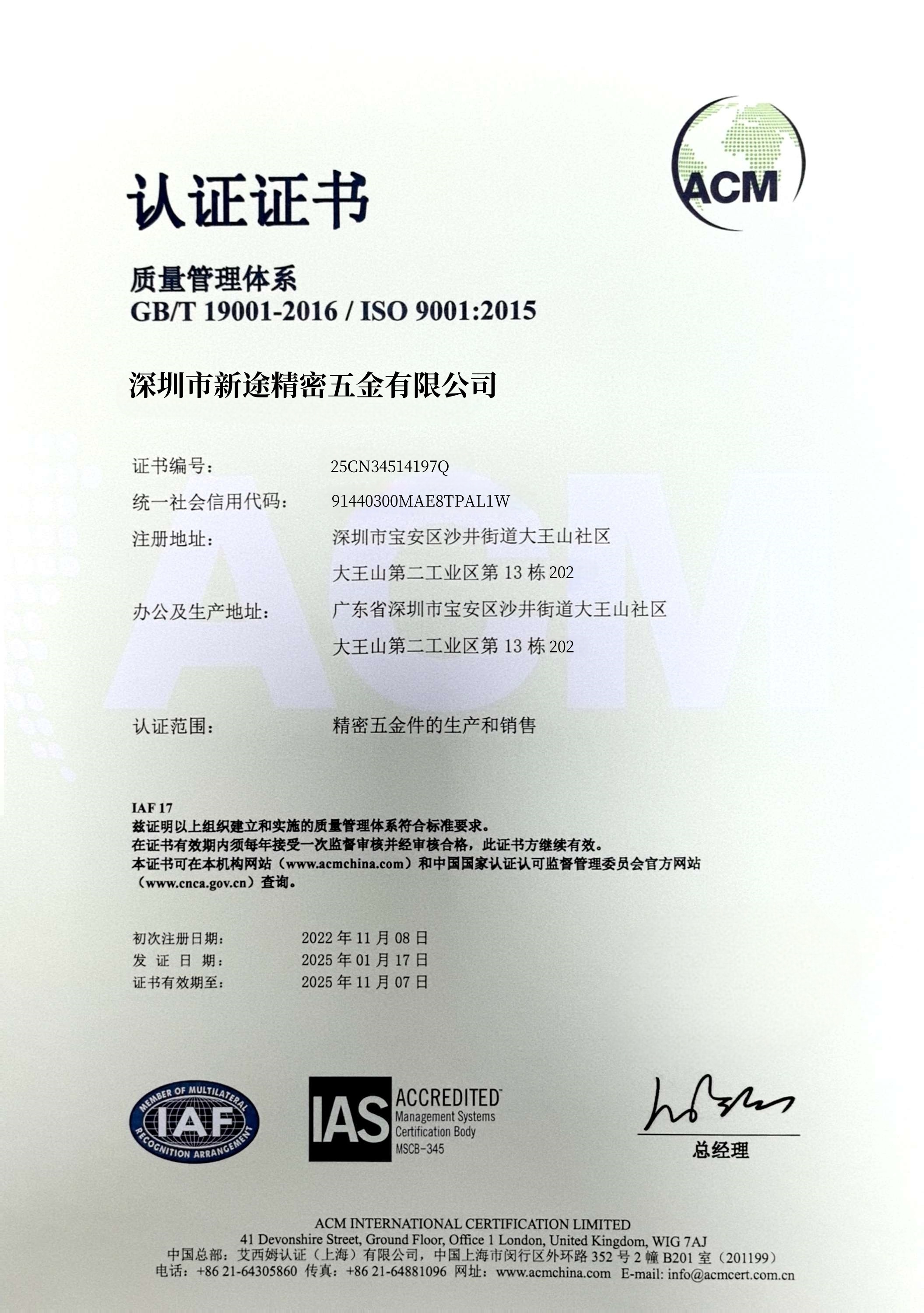
质量认证


Related Products

Shenzhen Nkeyto Precision Hardware Co., Ltd. is a factory specializing in precision hardware processing, committed to providing customers with high-quality products and services.We look forward to working with you.
Contact Us

E-mail: luna@nkeyto.com

Tel: +1 213-221-9094

Add: 13th Building, 202, Dawangshan Second Industrial Zone, Dawangshan Community, Shajing Street, Bao'an District, Shenzhen, Guangdong Province
Powered by: CEglobal
Copryright © 2025 Shenzhen Xintu Precision Hardware Co., Ltd.




Back To Top