



Chemical Etched RF Antenna Plate with Micro Pattern Design
Category:
Key Words:
Product parameters
Parameter | Specification / Range |
Product Name | RF Antenna Array Plate / Etched Antenna Plate / Metal Antenna Component |
Material | Stainless Steel / Copper / Brass / Aluminum / Nickel Alloy |
Thickness | 0.05 – 1.0 mm (customizable) |
Outer Diameter / Size | Custom according to drawing |
Aperture / Pattern Type | Etched slots / Micro apertures / Array patterns / Custom geometry |
Pattern Accuracy | High precision etched pattern |
Minimum Line Width | 0.03 – 0.10 mm (depending on material and thickness) |
Minimum Slot Width | 0.03 – 0.10 mm (customizable) |
Tolerance | ±0.005 – ±0.02 mm |
Surface Treatment | Cleaning / Passivation / Polishing / Nickel Plating / Tin Plating |
Edge Condition | Burr-free / Smooth edge |
Flatness | According to design requirement |
Manufacturing Process | Chemical Etching / Laser Cutting / Stamping / Forming |
Frequency Application | RF / Microwave / High Frequency / Communication Systems |
Structure Type | Flat plate / Array plate / Functional metal component |
OEM / ODM | Supported |
Drawing Format | PDF / CAD / DWG / DXF / STEP |
Sample | Available |
Lead Time | 5 – 15 days for samples, depending on complexity |
Packaging | Standard export packaging / Custom protective packaging |
Product Description
Product Description
Chemical etched RF antenna plate featuring micro pattern design for high-frequency signal transmission. The precision etching process ensures fine geometry, burr-free edges, and consistent dimensional accuracy, making it ideal for RF antenna and communication components. This etched antenna plate supports complex pattern customization and high-performance requirements.
Application Field
Used in RF antenna systems, communication equipment, electronic modules, and precision signal transmission devices. Suitable for applications requiring micro pattern RF plates and high accuracy etched components.
Precision Chemical Etched Antenna Plates with Micro-Patterns
In the realm of high-frequency electronics, the physical geometry of an antenna is just as critical as its electrical design. As devices become smaller and frequencies climb higher, the demand for microscopic precision increases. Our precision chemical etched antenna plates are engineered to meet these exacting standards, utilizing advanced subtractive manufacturing to create complex micro pattern plates that traditional methods simply cannot achieve.
We specialize in transforming raw metal sheets into functional RF components with micron-level accuracy. By leveraging chemical etching, we provide antenna manufacturers with burr-free, stress-free, and highly complex metal structures essential for modern communication systems.
The Superiority of Chemical Etching for Micro Patterns
Chemical etching, often referred to as photochemical machining, is a process that uses corrosive chemicals to dissolve unwanted material, leaving behind the precise structure defined by your design. Unlike mechanical cutting, which pushes against the metal, etching is a "cold" process that preserves the material's inherent properties.
For an RF engineer, the advantages of a chemical etched antenna are significant:
- Burr-Free Edges: Mechanical punching or milling often leaves microscopic burrs (raised edges) that can concentrate electric fields, leading to signal arcing or loss. Our etching process produces perfectly smooth edges, ensuring signal integrity.
- Zero Mechanical Stress: Stamping or CNC machining induces stress into the metal, which can cause warping or deformation over time. Etching leaves the metal flat and stress-free, which is vital for maintaining consistent impedance.
- Micro-Precision: We can achieve apertures and line widths as small as 0.1mm. This allows for the creation of dense micro-patterns required for high-gain antennas and miniaturized RF modules.
Etching vs. Traditional Manufacturing: A Technical Comparison
When designing a micro pattern plate for RF applications, the choice of manufacturing process dictates the design limits. Here is how our chemical etching process compares to traditional methods for complex antenna components.
Feature | Chemical Etching (Our Process) | Stamping / Punching | CNC Machining |
|---|---|---|---|
Edge Quality | Burr-free & Smooth (Ideal for RF) | Burrs present (Requires deburring) | Tool marks/roughness possible |
Material Stress | Zero Stress (Cold process) | High Stress (Cold working) | Thermal/Mechanical stress |
Complexity | High (Complex feeds/slots easy) | Low (Simple shapes only) | Medium (Limited by tool access) |
Lead Time | Fast (Digital tooling) | Slow (Hard tooling required) | Slow (Programming/Setup) |
Cost | Low for Prototypes | High initial tooling cost | High per-unit cost |
Designing Complex Feed Networks and U-Slots
One of the distinct advantages of our process is the ability to manufacture complex geometries without the constraints of physical tooling.
- Complex Feed Networks: Modern antennas often require intricate corporate feed networks to distribute signals across an array. Etching allows us to produce these fine lines and tight spaces in a single operation, ensuring uniform conductivity.
- U-Slots and E-Shapes: To enhance bandwidth or achieve circular polarization, antenna elements often feature U-slots or E-shaped patches. These difficult internal cuts are standard for our etching process, allowing for designs that would be impossible to stamp without expensive multi-stage dies.
Case Study: Microstrip Patch Antenna Array
To illustrate the capability of our precision etched antenna plates, consider a recent application involving a microstrip patch antenna array for a wireless communication module.
The client required a high-density array with a complex feed network on a thin copper substrate. Traditional stamping caused warping that detuned the frequency, while laser cutting was too slow for the required volume.
By utilizing our chemical etching process, we achieved:
- Dimensional Accuracy: Maintained a tolerance of ±0.01mm across the entire array.
- Surface Integrity: The etching process ensured the surface roughness was minimized, reducing the skin effect losses at high frequencies.
- Result: The client received a high-performance chemical etched antenna component that met their frequency specifications with minimal insertion loss, ready for immediate integration.
Materials and Surface Finishes
We work with a variety of conductive materials to suit your specific frequency and environmental requirements:
- Copper: Excellent conductivity, ideal for the radiating elements.
- Aluminum: Lightweight, suitable for structural antenna plates.
- Stainless Steel: High strength and corrosion resistance for harsh environments.
- Brass: Good machinability and conductivity for specific RF applications.
Have a complex design that traditional manufacturing can't handle?
Upload your CAD files today for a free feasibility assessment. Let us show you how chemical etching can optimize your antenna performance.
Contact Person: Luna
WhatsApp: 12132219094
Questions and Answers
Frequently Asked Questions
What is the minimum feature size you can etch?
We can achieve apertures and line widths as small as 0.1mm. This high precision makes our process ideal for creating the fine geometries required in micro pattern plates and high-frequency circuits.
Can you etch antennas on flexible materials?
Yes. Because chemical etching is a low-stress process, it is perfectly suitable for flexible substrates and thin laminates often used in flexible electronics and conformal antennas.
How does etching improve antenna performance?
By eliminating burrs and maintaining a smooth conductor surface, etching reduces the "skin effect" resistance that occurs at high frequencies. This results in lower signal loss and better overall efficiency for the chemical etched antenna.
Factory Description
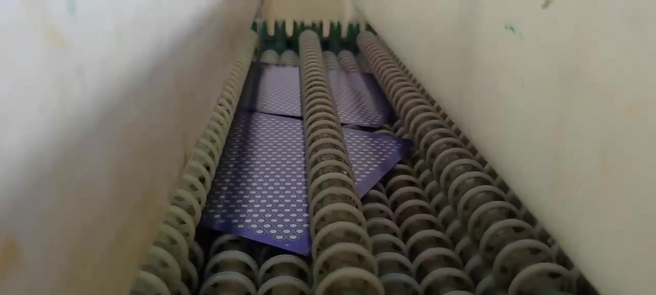
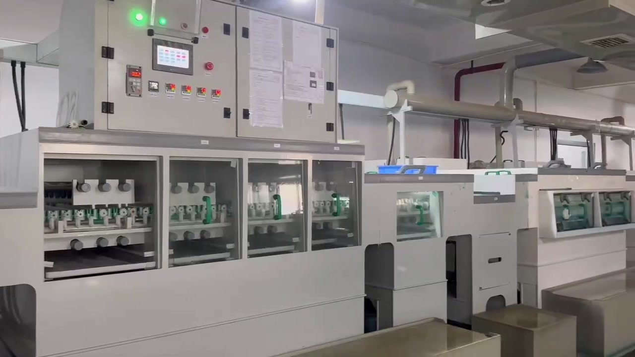
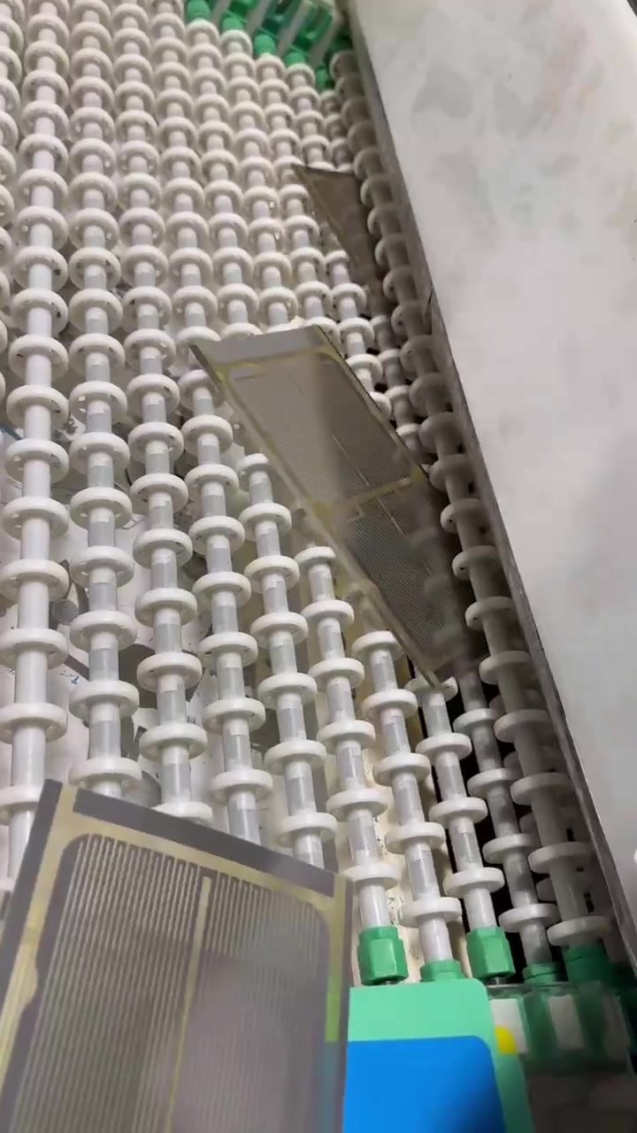
We have a full set of etching production equipment and mature processing technology. We can manufacture products in any shape with mesh sizes as small as 0.1mm, according to your requirements.

Our Advantage
Factory Direct Shipping
Our products undergo 100% QC checks before shipment, and we ensure compliance with international standards. If you require specific certifications for your target market, just let us know, and we'll meet those requirements.
Experienced Design and Manufacturing Team
We work closely with customers from the design phase to help avoid potential product flaws, ensuring both the functionality and design meet expectations.
Excellent Supply Chain Management
We can quickly adjust production schedules to meet your urgent deadlines, whether it's for large bulk orders or smaller rush orders.
OEM & ODM Support
We offer the option to print your logo or other customizations.
Strict Quality Control
Our products undergo 100% QC checks before shipment, and we ensure compliance with international standards. If you require specific certifications for your target market, just let us know, and we'll meet those requirements.
Certificate
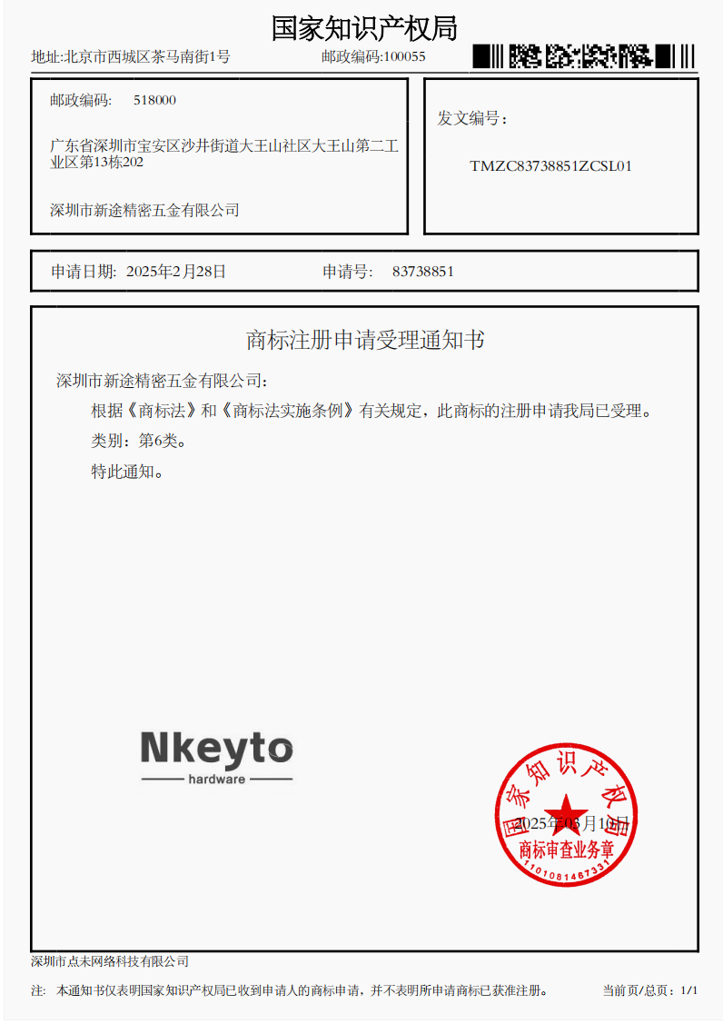
商标6类

9001
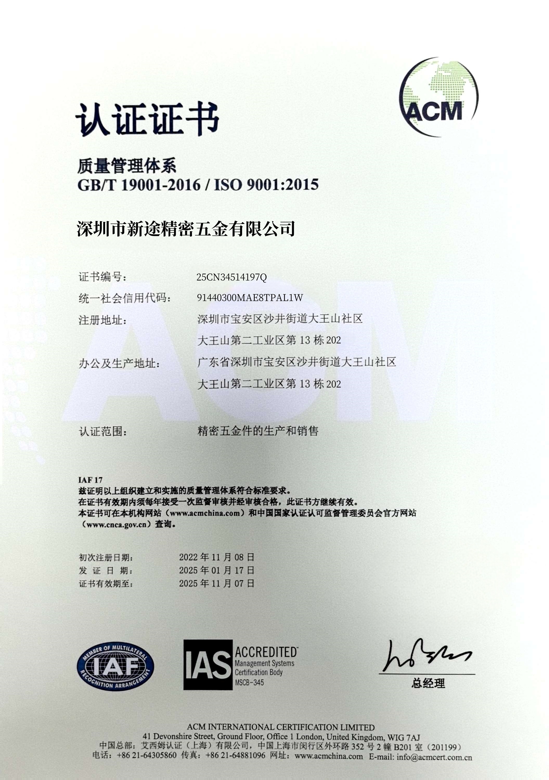
质量认证


Related Products

Shenzhen Nkeyto Precision Hardware Co., Ltd. is a factory specializing in precision hardware processing, committed to providing customers with high-quality products and services.We look forward to working with you.
Contact Us

E-mail: luna@nkeyto.com

Tel: +1 213-221-9094

Add: 13th Building, 202, Dawangshan Second Industrial Zone, Dawangshan Community, Shajing Street, Bao'an District, Shenzhen, Guangdong Province
Powered by: CEglobal
Copryright © 2025 Shenzhen Xintu Precision Hardware Co., Ltd.




Back To Top