



EMI Shielding Can Stainless Steel PCB RF Shield Cover
Category:
Key Words:
Product parameters
Parameter | Specification |
Product Name | EMI Shielding Can / RF Shielding Cover / PCB Shielding Can |
Material | Stainless Steel (SUS304 / SUS301), Nickel Silver, Copper |
Thickness | 0.05 mm – 0.30 mm |
Manufacturing Process | Chemical Etching + Stamping + Bending |
Surface Treatment | Tin Plating / Nickel Plating / Gold Plating / Natural Finish |
Shielding Effectiveness | 30 dB – 90 dB (depending on design & frequency) |
Frequency Range | MHz – GHz |
Dimensional Tolerance | ±0.01 – ±0.03 mm |
Flatness | ≤ 0.05 mm |
Hole Size | ≥ 0.03 mm (etching dependent) |
Structure Type | One-piece / Two-piece (Frame + Cover) / Clip Type |
Mounting Method | SMT Soldering / Through-hole / Clip-on |
Edge Condition | Burr-free (etching process) |
Operating Temperature | -40°C to 300°C (depending on material) |
Corrosion Resistance | High (optional plating for enhanced protection) |
Application Level | PCB Level / Module Level Shielding |
Customization | Size / Thickness / Hole Pattern / Structure / Surface Treatment |
Standards | RoHS / REACH compliant |
Product Description
Product Introduction:
This EMI shielding can is a precision stainless steel can designed for PCB-level electromagnetic interference protection. The RF shielding can effectively isolates high-frequency signals and reduces EMI noise, ensuring stable circuit performance. This PCB shielding can is widely used in communication modules and compact electronic devices where reliable signal integrity is required.
Applications:
WiFi modules, Bluetooth modules, smartphone PCB shielding, RF communication boards, compact electronic circuits
In the relentless pursuit of miniaturization within the electronics industry, the demand for high-precision EMI Shielding Cans has never been greater. These components—often referred to as RF Shields or PCB Shields—are critical for maintaining signal integrity in high-frequency environments.
When it comes to manufacturing these enclosures, engineers face a choice: traditional stamping, laser cutting, or chemical etching. While all methods produce a metal box, the structural and surface quality differ significantly. For applications requiring the highest reliability, our engineering team consistently recommends the photochemical etching process.
Here is why chemical etching is the superior solution for modern Precision RF Shielding.
The "Burr-Free" Advantage: Protecting Sensitive PCBs
One of the most critical issues with stamped Metal Shielding Cans is the formation of burrs. Mechanical punching shears the metal, leaving sharp, raised edges.
- The Problem: During the assembly of a PCB Shielding Can, these burrs can break off. Loose metal particles (often called "nesting") on a circuit board are a primary cause of short circuits.
- Our Solution: Our chemical etching process works by uniformly dissolving the metal. Because there is no physical force involved, the resulting parts are completely burr-free.
- The Result: You receive a Stainless Steel Can with perfectly smooth edges, eliminating the risk of contamination on sensitive boards.
Stress-Free Processing: Eliminating Warpage
Maintaining flatness is crucial for an EMI Shielding Cover to make proper contact with the PCB gasket.
- The Problem: Stamping is a high-force process. This "cold working" of the metal introduces internal stresses. Over time, or when exposed to temperature fluctuations (common in automotive or industrial electronics), these stresses can cause the metal to warp or deform (No Stress Deformation is key here).
- Our Solution: Chemical etching is a non-contact, thermal-neutral process. The molecular structure of the metal remains unchanged.
- The Result: Our RF Shielding Cans remain perfectly flat throughout their lifecycle, ensuring consistent grounding and reliable EMC (Electromagnetic Compatibility) performance.
Precision at the Micro Level: 0.1mm Apertures
As devices shrink, the need for intricate venting patterns without compromising structural rigidity has increased.
- The Challenge: Laser cutting can achieve small holes, but the heat-affected zone (HAZ) can alter the magnetic properties of the shielding material. Stamping tiny holes is expensive and prone to tool breakage.
- Our Capability: Our factory specializes in high-resolution photo-tooling. We can consistently produce Fine Structure features, including apertures as small as 0.1mm.
- The Result: This allows for complex Etched Metal patterns that provide optimal airflow for heat dissipation while maintaining the shielding effectiveness required for 5G and high-frequency RF modules.
Process Comparison: Why Choose Etching?
To help you evaluate the best method for your next Custom Shielding Can, here is a technical comparison:
表格
Feature | Stamping (Punching) | Laser Cutting | Chemical Etching (Our Process) |
|---|---|---|---|
Edge Quality | High burr formation | Sharp edges, potential HAZ | Burr-free, smooth edges |
Material Integrity | Work-hardened, stressed | Thermally stressed edges | Stress-free, original grain structure |
Tooling & Cost | High cost, long lead time | Low cost | Low cost, digital tooling |
Design Flexibility | Hard to modify | Easy to modify | Easy to modify (film-based) |
Minimum Feature | Limited by punch strength | Limited by beam width | 0.1mm Micro features achievable |
Applications Where Our Process Excels
Our process is engineered for the most demanding environments:
- High-Density PCB Shielding: Where even a microscopic burr can cause a failure.
- 5G Communication Modules: Requiring the tight tolerances and fine features only possible with etching.
- Automotive Electronics: Where thermal cycling demands No Stress Deformation to prevent seal failure.
- Rapid Prototyping: Since our "tooling" is a digital film, we can produce Custom EMI Shielding Covers in days, not weeks.
Whether you need a simple RF Shielding Cover or a complex Etched Metal Enclosure with integrated clips and micro-perforations, our process ensures dimensional consistency and superior shielding performance.
Ready to Optimize Your Design?
If you are currently facing yield issues with stamped shields or need to push the limits of miniaturization, our engineering team is ready to assist.
Contact us to discuss your requirements for Precision Etched Metal Components or to request a quote for your next project.
- Contact Person: Luna
- WhatsApp: 12132219094
Questions and Answers
Frequently Asked Questions (FAQ)
Q1: What materials are best suited for etched RF shields?
While we process various alloys, Stainless Steel is the most popular choice for our Precision RF Shield clients. It offers the perfect balance of corrosion resistance, durability, and magnetic permeability. However, we also frequently process Copper and Phosphor Bronze for specific conductivity needs.
Q2: Can etching produce 3D shapes, or just flat parts?
Chemical etching is primarily a 2D process used to create flat blanks. However, our factory combines this with secondary CNC forming operations. This hybrid approach allows us to create complex 3D Metal Shielding Cans that retain the precision edges of the etched blank, offering the best of both worlds.
Q3: What is the tolerance for a 0.1mm hole?
Achieving a 0.1mm aperture requires strict process control. Our standard etching tolerance is typically ±0.025mm to ±0.05mm, depending on the material thickness. For critical features in a Fine Structure Cover, we recommend designing with these tolerances in mind to ensure the final fit.
Q4: Is chemical etching cost-effective for mass production?
Yes. Although often associated with prototyping due to low tooling costs, our production lines are optimized for high volume. Because the etching "tool" is a digital photo-tool (which never wears out), we maintain consistent quality over millions of parts—making it ideal for OEM manufacturing.
Factory Description
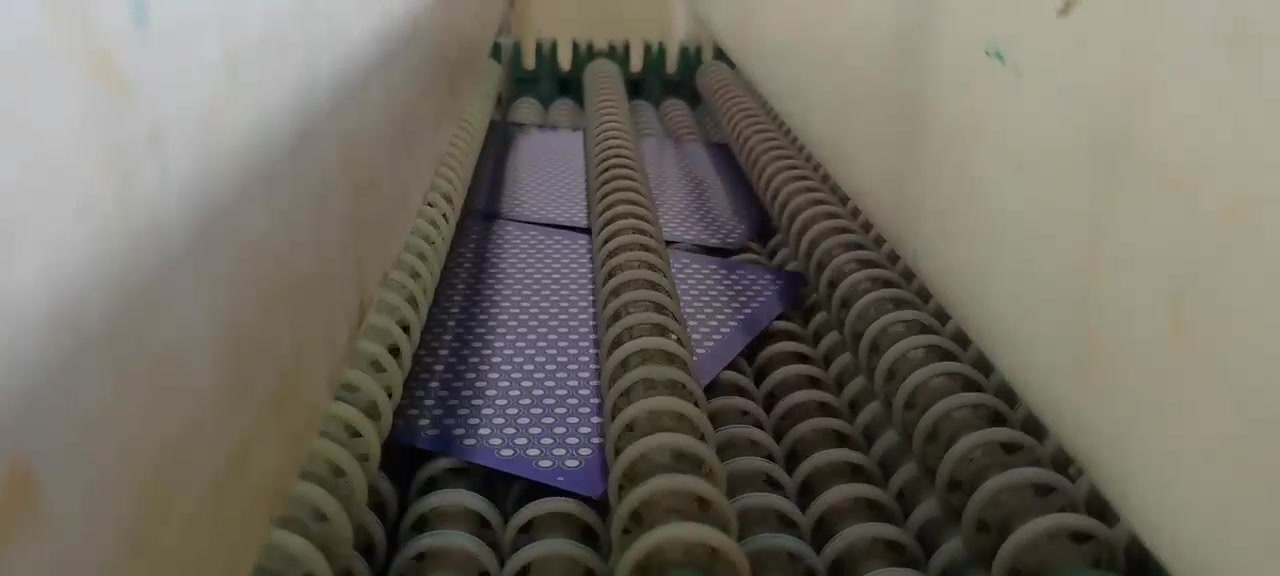
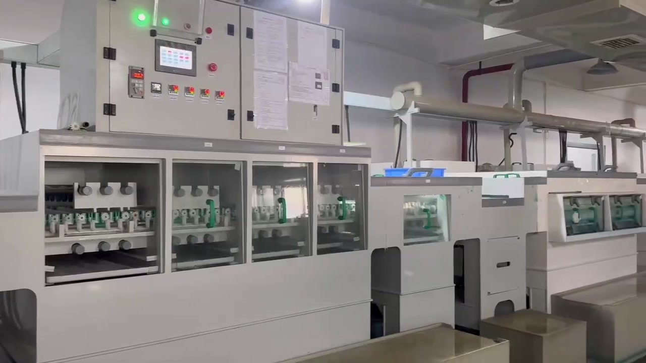
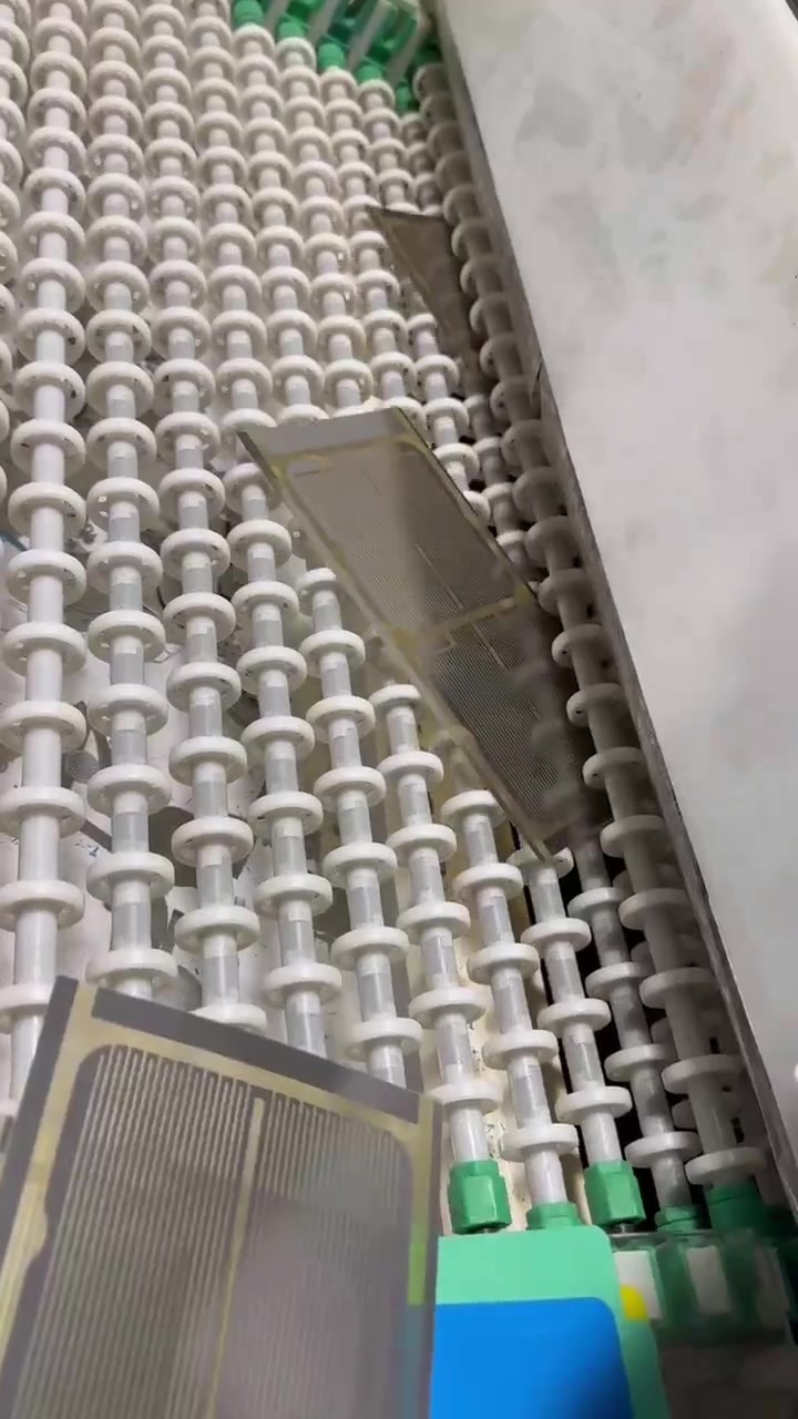
We have a full set of etching production equipment and mature processing technology. We can manufacture products in any shape with mesh sizes as small as 0.1mm, according to your requirements.

Our Advantage
Factory Direct Shipping
Our products undergo 100% QC checks before shipment, and we ensure compliance with international standards. If you require specific certifications for your target market, just let us know, and we'll meet those requirements.
Experienced Design and Manufacturing Team
We work closely with customers from the design phase to help avoid potential product flaws, ensuring both the functionality and design meet expectations.
Excellent Supply Chain Management
We can quickly adjust production schedules to meet your urgent deadlines, whether it's for large bulk orders or smaller rush orders.
OEM & ODM Support
We offer the option to print your logo or other customizations.
Strict Quality Control
Our products undergo 100% QC checks before shipment, and we ensure compliance with international standards. If you require specific certifications for your target market, just let us know, and we'll meet those requirements.
Certificate
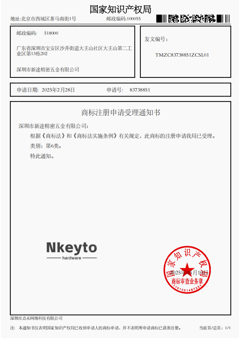
商标6类

9001
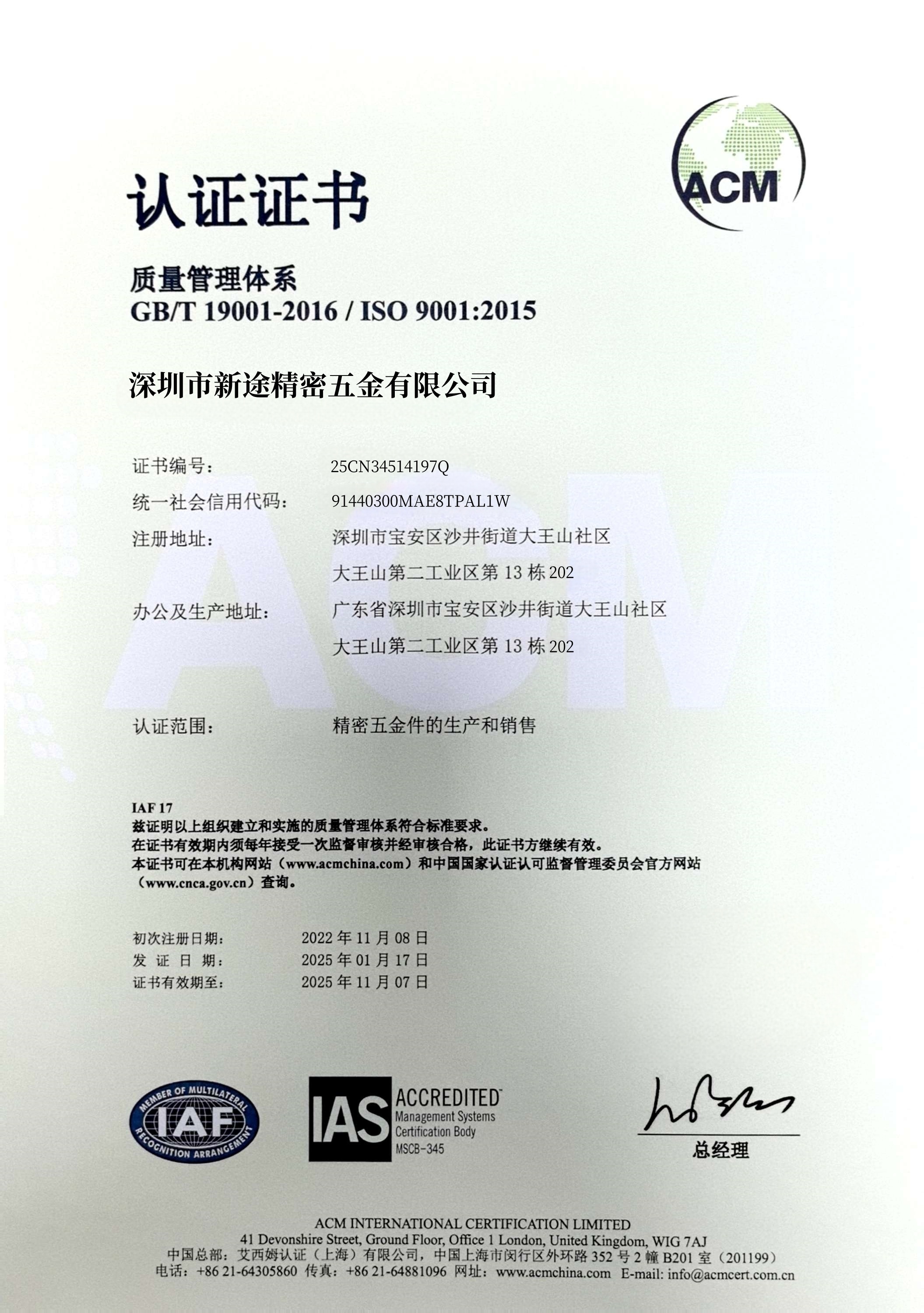
质量认证


Related Products

Shenzhen Nkeyto Precision Hardware Co., Ltd. is a factory specializing in precision hardware processing, committed to providing customers with high-quality products and services.We look forward to working with you.
Contact Us

E-mail: luna@nkeyto.com

Tel: +1 213-221-9094

Add: 13th Building, 202, Dawangshan Second Industrial Zone, Dawangshan Community, Shajing Street, Bao'an District, Shenzhen, Guangdong Province
Powered by: CEglobal
Copryright © 2025 Shenzhen Xintu Precision Hardware Co., Ltd.




Back To Top