



Etched Metal Contact Strip
Category:
Key Words:
Product parameters
Parameter | Description |
Material | Stainless Steel (SUS301 / SUS304 / SUS316), Beryllium Copper (optional), Phosphor Bronze (optional) |
Manufacturing Process | Chemical Etching (Primary), Forming / Bending (Optional), Laser Cutting (Auxiliary) |
Shape | Flat / Spring type / Cantilever / Multi-contact / Custom profiles |
Size Range | Customizable (Typical: ≤ 300 × 300 mm) |
Thickness | 0.01 mm – 0.5 mm (Etching optimal: 0.02–0.3 mm) |
Hole Diameter (if applicable) | ≥ 0.05 mm |
Minimum Line Width | ≥ 0.03 mm |
Tolerance | ±0.005 mm ~ ±0.02 mm |
Etching Accuracy | ±10% of material thickness |
Elastic Property | Available in half-hard / full-hard materials (SUS301 / copper alloys) |
Contact Force | Customizable based on design and material |
Edge Quality | Burr-free, smooth edge, no deformation |
Flatness | ≤ 0.03 mm |
Surface Finish | Nickel Plating / Gold Plating / Tin Plating / Passivation (optional) |
Conductivity | High conductivity (especially copper alloys) |
Customization (OEM/ODM) | Supported (based on drawings or samples) |
Drawing Formats Accepted | CAD / DWG / DXF / STEP / PDF |
Quality Control | Dimensional inspection, spring force testing (optional), plating thickness inspection |
Product Description
Product Description:
Etched metal contact strip is a continuous precision metal strip with fine etched structures, designed for high-density electronic assemblies. This contact strip is produced using chemical etching or laser cutting, offering high dimensional consistency, smooth edges, and excellent repeatability. It is suitable for reel-to-reel production and automated assembly processes.
Key Features:
Connector strip manufacturing
Electronic assembly lines
Sensor contact structures
Micro metal strip components
Precision stamped or etched strip parts
Enhancing Signal Integrity in High-Density Connectors with Etched Contact Strips
The telecommunications and data industries are currently navigating a massive shift toward 5G infrastructure and high-speed data transmission. As devices become smaller and data rates skyrocket, the components inside them must evolve. The humble connector, once a simple mechanical interface, has become a critical bottleneck for signal performance.
In this high-stakes environment, the manufacturing method of the internal contacts determines the success of the entire assembly. For engineers designing next-generation hardware, the Connector contact strip is the foundation of reliability. Our factory addresses the challenges of modern connectivity by utilizing precision chemical etching to produce High-density connector solutions that outperform traditional stamped parts.
The Challenge: The Density vs. Integrity Trade-Off
Modern electronics demand two conflicting things: miniaturization and massive bandwidth. As engineers pack more pins into smaller connectors to support 5G and PCIe Gen 5/6 standards, the "pitch" (the distance between pins) shrinks.
When pitch decreases, the margin for error disappears. A microscopic burr from a stamping die can cause a short circuit between adjacent pins. Furthermore, at high frequencies, signal integrity is paramount. Any variation in the metal's thickness or surface roughness can cause impedance mismatches, leading to signal reflection and data loss.
Key Challenges in High-Speed Design:
- Signal Loss: The need for Signal integrity metal parts that maintain consistent impedance.
- Physical Space: Connectors must be incredibly compact, requiring thinner and more precise metal contacts.
- Assembly Speed: Manufacturers need components that work flawlessly in automated reel-to-reel assembly lines.
The Solution: Precision Etched Metal Contact Strips
Traditional stamping struggles when features become too small or complex. The physical force of the die distorts the metal, creating stress points and "roll-over" edges. Chemical etching, conversely, is a subtractive process that removes material without force.
Our Etched Metal Contact Strip is manufactured using a digital photo-tool. This allows us to create complex lead frames and contact geometries that are impossible with hard tooling. Because the process is digital, there is no tool wear, meaning the first part in the reel is identical to the millionth part.
Why Etched Strips Win for High Density:
- Zero Burrs: Etching produces smooth, burr-free edges, eliminating the risk of shorting between tightly packed pins.
- Half-Etching Capability: We can selectively reduce thickness in specific areas. This allows a single strip to have rigid mounting tabs and flexible, spring-like contact fingers, all in one piece.
- Perfect Flatness: Without the mechanical stress of stamping, the metal strip remains perfectly flat, which is essential for maintaining the precise air gaps required for controlled impedance.
NKEYTO: Engineered for Automation and Consistency
We understand that our components are just one part of a larger automated assembly process. Our clients use high-speed pick-and-place machines and reel-to-reel plating lines. Therefore, consistency is not just a quality metric; it is a functional requirement.
At our Shenzhen facility, we produce Connector contact strips that are optimized for this environment. We control the carrier tape design and the tie-bar locations to ensure the strip feeds smoothly through automated equipment without jamming or warping.
Our Production Capabilities:
- Material Versatility: We process high-performance alloys like Beryllium Copper and Phosphor Bronze, which are essential for maintaining spring force in miniature contacts.
- Tight Tolerances: We hold tolerances as tight as ±0.01mm, ensuring that every contact aligns perfectly within the connector housing.
- Scalability: From prototyping digital designs to mass production, our etching lines are built to deliver high volumes without compromising the precision required for Signal integrity metal parts.
Conclusion
As the industry moves toward 112Gbps and beyond, the quality of the physical connection is more critical than ever. Stamping is reaching its physical limits in the realm of micro-connectivity. By switching to precision-etched contact strips, designers can achieve the density and signal purity required for modern 5G and data center applications.
Ready to Optimize Your Connector Design?
If you are facing challenges with signal integrity or connector miniaturization, our team is ready to help. We specialize in high-precision solutions for the 5G and data industries. Contact Luna on WhatsApp at 12132219094 to discuss your High-density connector solutions and request a quote today.
Questions and Answers
Frequently Asked Questions (FAQ)
Q: What is the minimum pitch you can achieve with an etched contact strip?
A: Chemical etching allows us to achieve extremely fine pitches, often down to 0.15mm or less, depending on the material thickness. This makes it ideal for micro-connectors.
Q: Can you produce strips that are suitable for reel-to-reel plating?
A: Yes. We design our Etched Metal Contact Strips with specific carrier rails and tie-bars to ensure they are robust enough for high-speed reel-to-reel plating and automated assembly.
Q: How does etching improve signal integrity compared to stamping?
A: Etching produces a smoother surface finish and eliminates the micro-cracks and stress points caused by stamping. This reduces surface roughness, which minimizes signal loss (insertion loss) at high frequencies.
Q: Do you offer "half-etching" for creating 3D shapes in the strip?
A: Yes. We can etch away material on one side to create steps or thinned sections. This allows the strip to be bent or formed into complex 3D shapes while maintaining a single-piece construction.
Factory Description
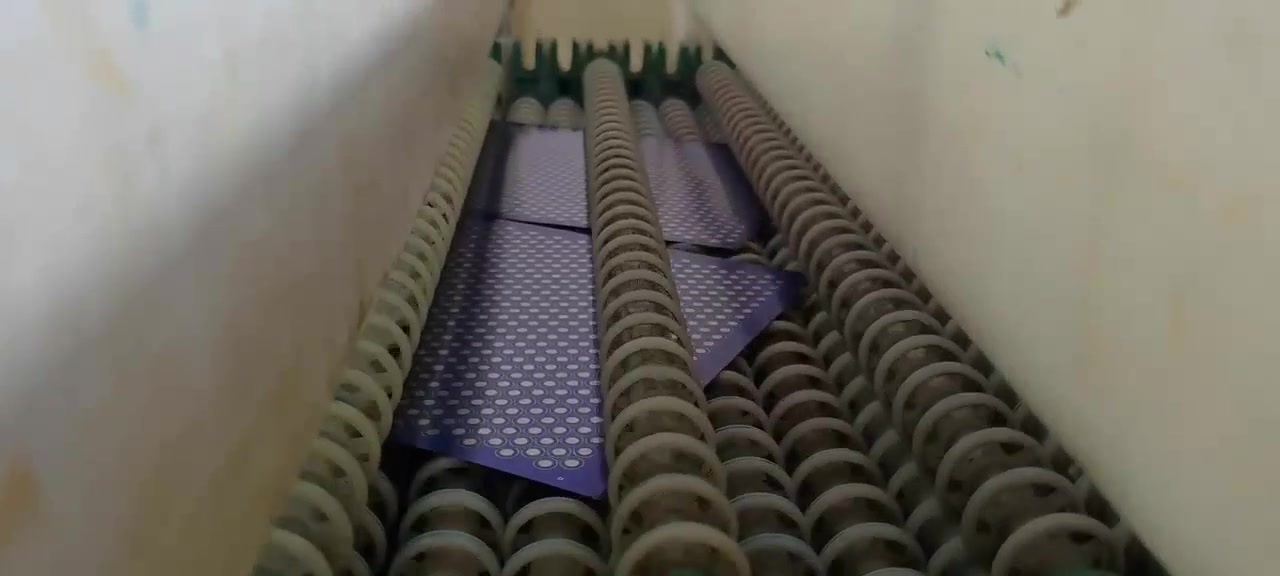
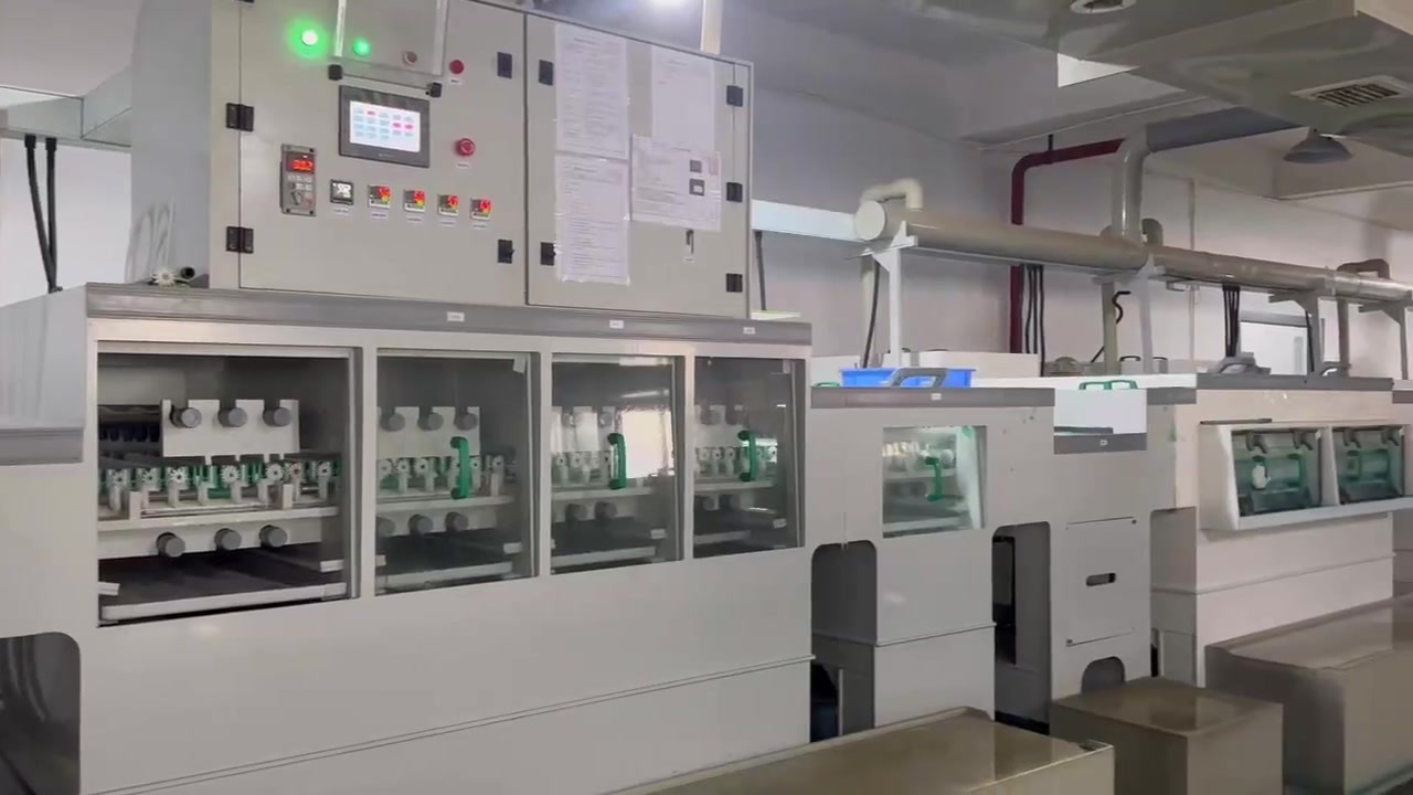
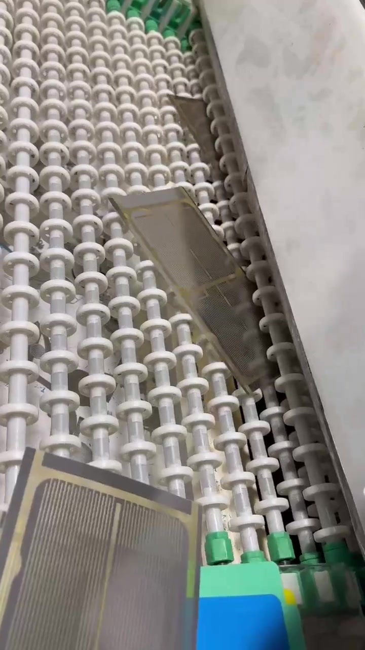
We have a full set of etching production equipment and mature processing technology. We can manufacture products in any shape with mesh sizes as small as 0.1mm, according to your requirements.

Our Advantage
Factory Direct Shipping
Our products undergo 100% QC checks before shipment, and we ensure compliance with international standards. If you require specific certifications for your target market, just let us know, and we'll meet those requirements.
Experienced Design and Manufacturing Team
We work closely with customers from the design phase to help avoid potential product flaws, ensuring both the functionality and design meet expectations.
Excellent Supply Chain Management
We can quickly adjust production schedules to meet your urgent deadlines, whether it's for large bulk orders or smaller rush orders.
OEM & ODM Support
We offer the option to print your logo or other customizations.
Strict Quality Control
Our products undergo 100% QC checks before shipment, and we ensure compliance with international standards. If you require specific certifications for your target market, just let us know, and we'll meet those requirements.
Certificate
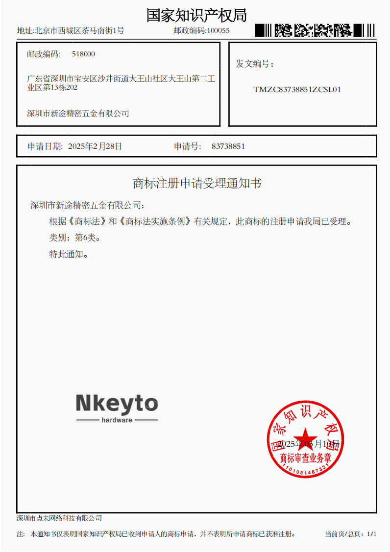
商标6类

9001
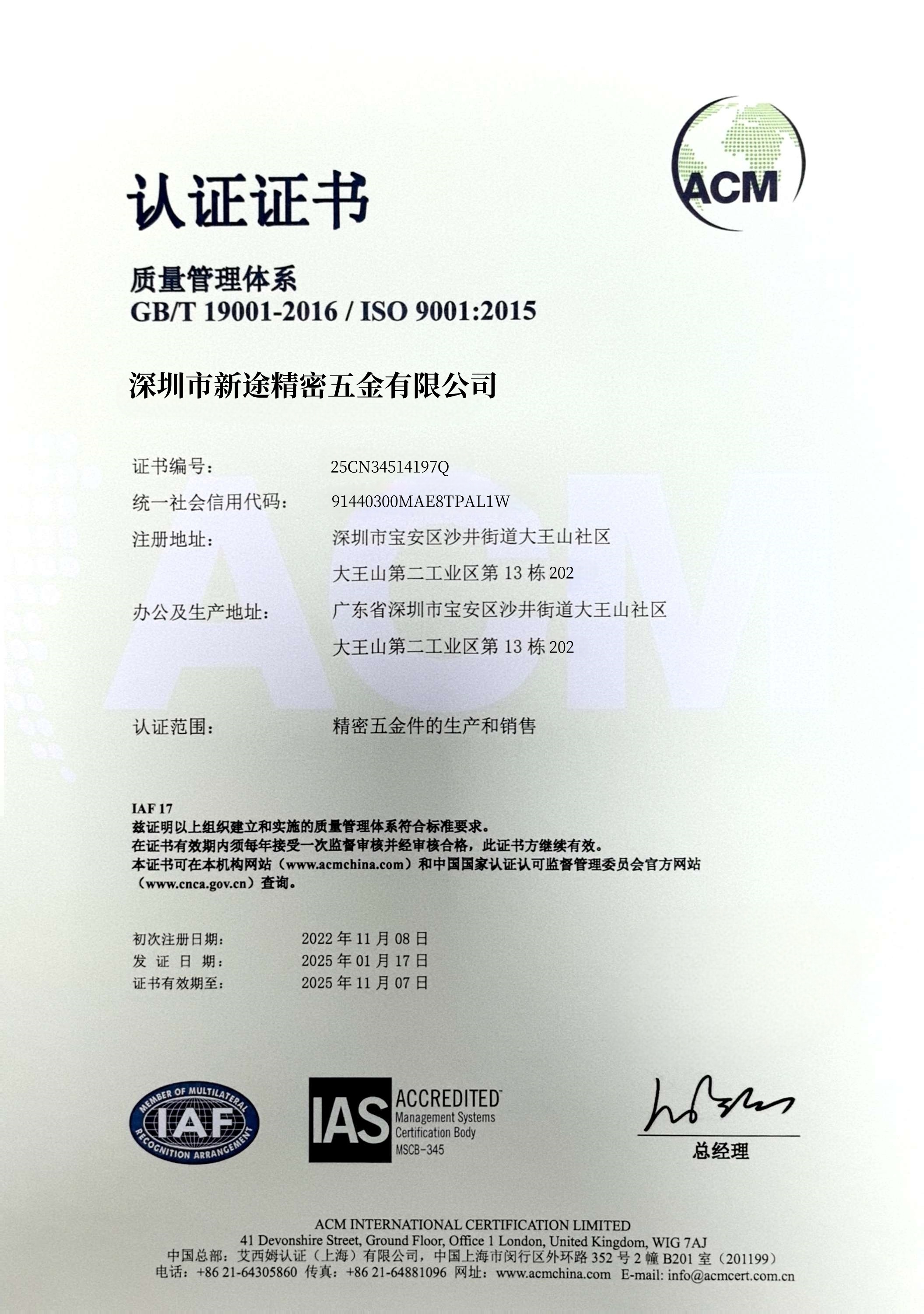
质量认证


Related Products

Shenzhen Nkeyto Precision Hardware Co., Ltd. is a factory specializing in precision hardware processing, committed to providing customers with high-quality products and services.We look forward to working with you.
Contact Us

E-mail: luna@nkeyto.com

Tel: +1 213-221-9094

Add: 13th Building, 202, Dawangshan Second Industrial Zone, Dawangshan Community, Shajing Street, Bao'an District, Shenzhen, Guangdong Province
Powered by: CEglobal
Copryright © 2025 Shenzhen Xintu Precision Hardware Co., Ltd.




Back To Top