



Precision Etched Copper Component for Electronic Applications
Category:
Key Words:
Product parameters
Parameter | Specification / Range |
Product Name | Etched Copper Sheet / Etched Copper Plate / Copper Component |
Material | Copper (C1100 / C1020) / Brass (optional) |
Thickness | 0.03 – 1.0 mm (customizable) |
Max Size | Up to 600 × 1500 mm (depending on material) |
Pattern Type | Micro holes / Slots / Complex etched patterns |
Minimum Feature Size | 0.03 – 0.10 mm (depending on thickness) |
Tolerance | ±0.005 – ±0.02 mm |
Edge Condition | Burr-free / Smooth edge |
Surface Treatment | Cleaning / Passivation / Polishing / Nickel plating / Tin plating |
Flatness | High precision control |
Manufacturing Process | Chemical Etching / Laser Cutting / Secondary Processing |
Conductivity | Excellent electrical conductivity (copper material) |
Structure Type | Flat sheet / Formed / Multi-layer |
Hole Type | Round / Square / Slot / Custom geometry |
Open Area | 10% – 70% (depending on design) |
OEM / ODM | Supported |
Drawing Format | PDF / CAD / DWG / DXF / STEP |
Sample | Available |
Lead Time | 5 – 15 days |
Packaging | Standard export packaging / Custom packaging |
Product Description
Product Description
Precision etched copper component designed for electronic applications requiring stable conductivity and accurate structural performance. Produced with high-precision etching processes, this copper component features fine patterns, consistent thickness, and reliable quality. It is suitable for applications where electrical performance and structural accuracy are critical.
Application Field
Widely used in electronic modules, connectors, sensors, and circuit-related components. This etched copper component is suitable for consumer electronics, communication devices, and industrial electronics.
Precision Etched Copper Component for Electronic Applications
For electronic applications demanding stable conductivity and precise structure, our precision etched copper component is the ideal solution. We ensure fine patterns and consistent thickness for reliable electrical performance. In an industry driven by miniaturization and high-speed data transmission, the integrity of your metal parts is non-negotiable.
Our factory specializes in manufacturing electronic precision metal components using advanced chemical etching technology. We bridge the gap between complex circuit design and physical manufacturing, delivering parts that offer superior flatness, zero burrs, and unaltered material properties.
Uncompromised Conductivity and Structural Integrity
Copper is the backbone of the electronics industry due to its superior conductivity. However, traditional machining methods can compromise these properties. Our precision etched copper components are manufactured to preserve the inherent qualities of the metal while achieving geometries that other methods cannot.
Why Electronics Engineers Choose Our Components
- Stable Conductivity: Chemical etching is a "cold" process. Unlike laser cutting, it generates no heat-affected zones (HAZ) that could alter the grain structure or resistance of the copper. This ensures your electronic components maintain consistent electrical performance.
- Accurate Structural Performance: Modern electronics require tight stacking and precise alignment. Our process guarantees exceptional flatness and dimensional stability, ensuring that connectors and contacts fit perfectly within the assembly.
- Complex Geometries: From fine-pitch lead frames to intricate EMI shielding grids, we can etch complex patterns with high definition. This allows for the miniaturization of electronic modules without sacrificing strength.
- Zero Burrs, Zero Short Circuits: In sensitive electronics, even microscopic metal shards can cause catastrophic failure. Our etching process produces smooth, burr-free edges, eliminating the risk of short circuits and ensuring reliability.
Applications in the Electronics Industry
Our etched copper components are engineered for performance in critical sectors. We provide tailored solutions for:
- Connectors and Terminals: High-precision contacts (often using C7025 or Beryllium Copper) that require exact spring properties and low contact resistance.
- Sensors: Delicate sensor elements where fine patterns and material integrity are critical for accurate signal transmission.
- Electronic Modules: EMI/RFI shielding cans and structural frames that protect sensitive circuitry from interference.
- Battery Technology: Precision busbars and contacts for lithium-ion batteries, ensuring efficient power distribution.
- Communication Devices: Components for 5G infrastructure and antennas requiring high-frequency performance and strict tolerances.
Process Comparison: The Etching Advantage
When selecting a manufacturing method for electronic precision metal components, the choice impacts both performance and cost.
Chemical Etching vs. Stamping
Stamping is a common method, but it exerts immense physical force on the metal.
- Material Stress: Stamping can deform thin copper and alter its temper (hardness). Our etching process is non-contact, meaning the copper retains its original ductility and electrical properties.
- Tooling Costs: Hard steel dies are expensive and slow to produce. We use digital photo tools, allowing for rapid design changes—crucial for the fast-paced electronics sector.
Chemical Etching vs. Laser Cutting
While lasers offer precision, they struggle with highly conductive metals like copper.
- Edge Quality: Lasers can leave recast layers or micro-burrs on the cut edge. For high-density assemblies, our chemical etching provides a cleaner edge profile, ensuring better contact and reducing the need for post-processing.
- Heat Damage: The heat from lasers can oxidize copper edges. Our chemical process leaves the material pristine and ready for plating.
Technical Capabilities for Electronics
We work with a variety of conductive alloys, including pure copper, phosphor bronze, and specialized connector alloys, to meet specific conductivity and strength requirements.
Feature | Specification |
|---|---|
Materials | Copper (C1100, C1020), Brass, C7025, C17200 (BeCu) |
Thickness | 0.03mm – 2.0mm |
Tolerance | ±0.01mm (Ideal for tight-fit connectors) |
Min. Aperture | 0.1mm (For fine mesh and shielding) |
Surface Finish | Tin, Nickel, Gold, Silver plating, or Passivation |
Quality Control and Manufacturing
As a manufacturer with over 10 years of experience, we employ strict quality control measures suitable for the high-reliability electronics industry.
- Material Traceability: We use only certified raw materials (RoHS/REACH compliant) to ensure consistent conductivity and chemical composition.
- Optical Inspection: Every precision etched copper component undergoes rigorous visual and dimensional inspection to detect any defects such as over-etching or pinholes.
- Plating Adhesion: For plated parts, we perform adhesion and solderability tests to ensure the coating withstands thermal cycling and mechanical stress.
Request Samples for Your Electronic Project
Ensure your electronic devices perform reliably with high-quality metal components. Whether you need simple contacts or complex shielding solutions, our team is ready to support your engineering needs.
Contact us today to discuss your specifications and request a quote.
- WhatsApp: +86 12132219094
- Factory Location: Shenzhen, China
Questions and Answers
Frequently Asked Questions (FAQ)
Q: Can you plate the copper components after etching?
A: Yes, we offer comprehensive surface treatments including tin, nickel, gold, and silver plating. This is essential for improving solderability and corrosion resistance in electronic applications.
Q: What is the benefit of etching for thin copper sheets?
A: Etching is the superior choice for thin sheets (under 2mm) as it prevents the warping and deformation often caused by stamping. It ensures the electronic precision metal components remain perfectly flat for assembly.
Q: Do you manufacture busbars or lead frames?
A: Yes, our chemical etching capabilities are perfectly suited for producing complex busbars and lead frames with high dimensional accuracy and no burrs.
Q: How fast can you produce prototypes for electronic parts?
A: We can typically produce samples within 3-5 days, allowing you to test the fit and electrical performance of your design quickly without waiting for hard tooling.
Q: Is chemical etching suitable for high-volume production?
A: Absolutely. While it is famous for rapid prototyping, it is also highly cost-effective for mass production, especially for complex parts where stamping dies would be too expensive or slow to maintain.
Factory Description
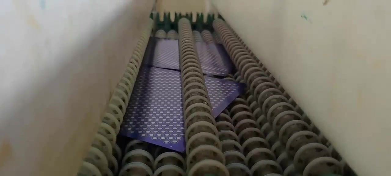
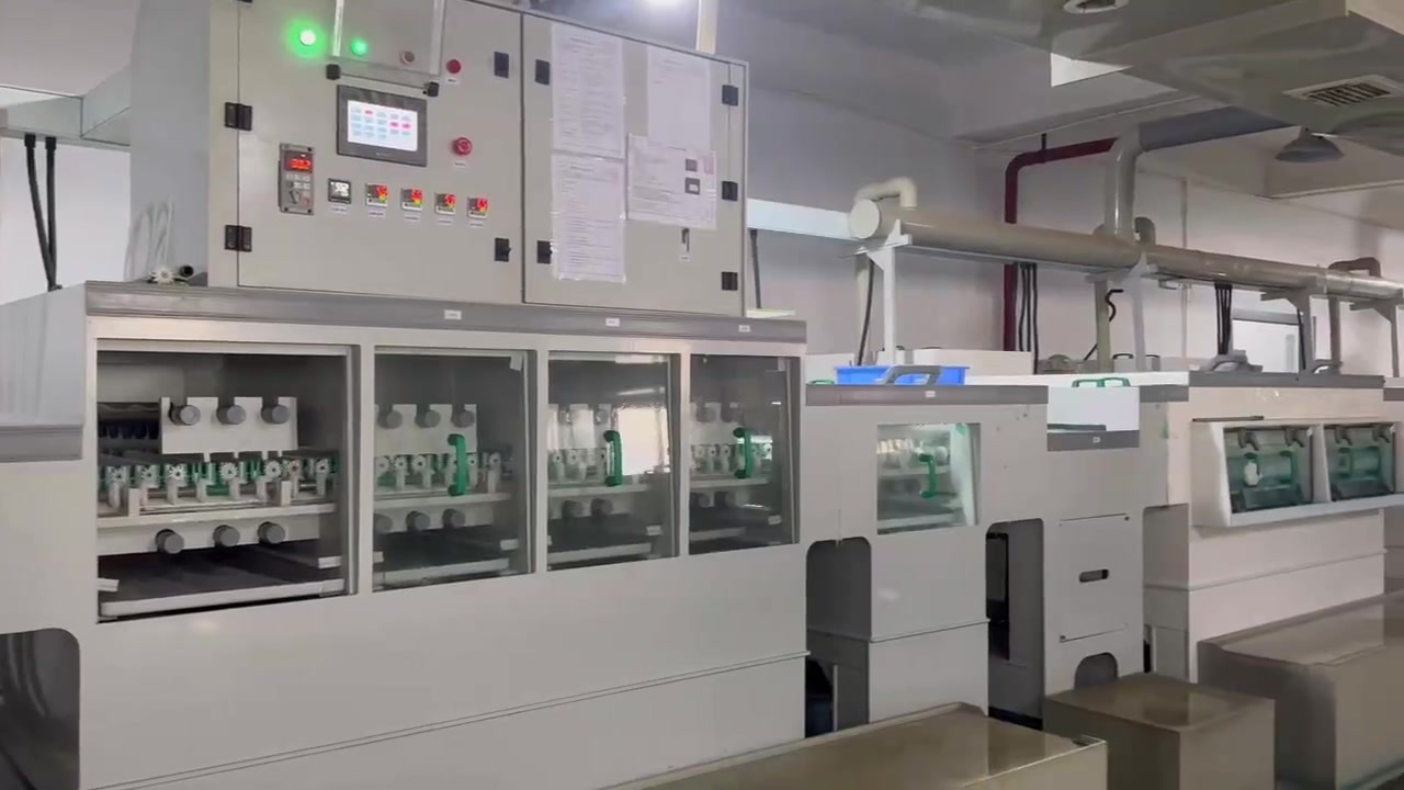
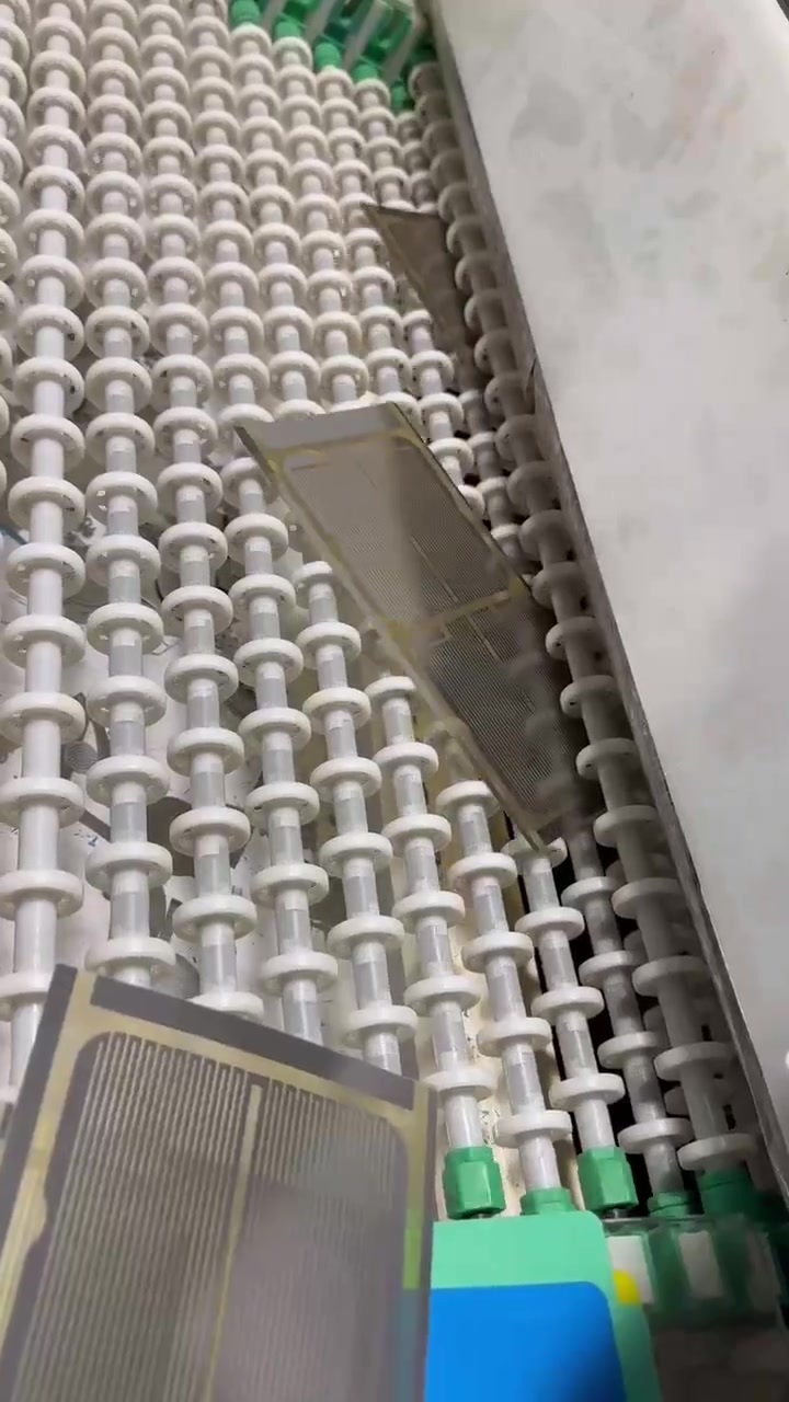
We have a full set of etching production equipment and mature processing technology. We can manufacture products in any shape with mesh sizes as small as 0.1mm, according to your requirements.

Our Advantage
Factory Direct Shipping
Our products undergo 100% QC checks before shipment, and we ensure compliance with international standards. If you require specific certifications for your target market, just let us know, and we'll meet those requirements.
Experienced Design and Manufacturing Team
We work closely with customers from the design phase to help avoid potential product flaws, ensuring both the functionality and design meet expectations.
Excellent Supply Chain Management
We can quickly adjust production schedules to meet your urgent deadlines, whether it's for large bulk orders or smaller rush orders.
OEM & ODM Support
We offer the option to print your logo or other customizations.
Strict Quality Control
Our products undergo 100% QC checks before shipment, and we ensure compliance with international standards. If you require specific certifications for your target market, just let us know, and we'll meet those requirements.
Certificate
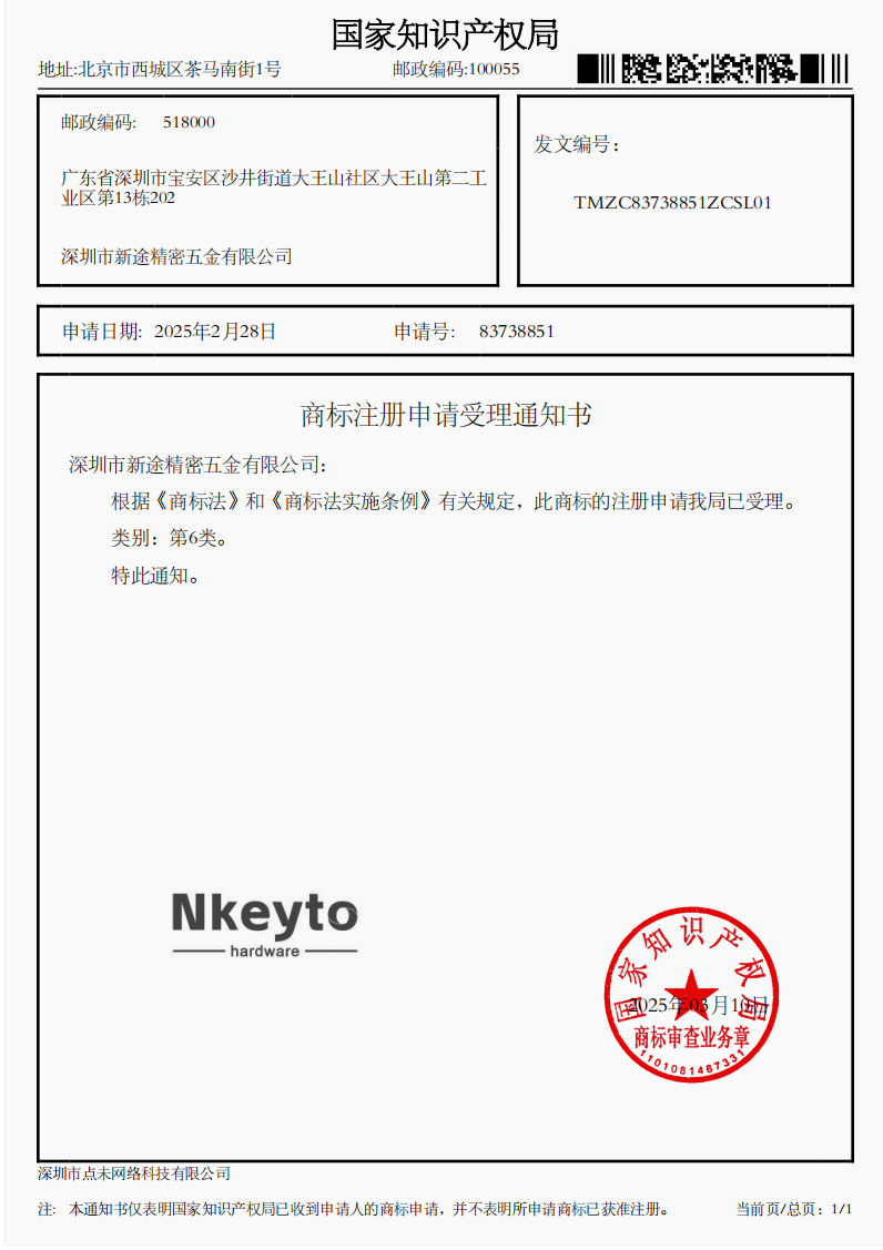
商标6类

9001
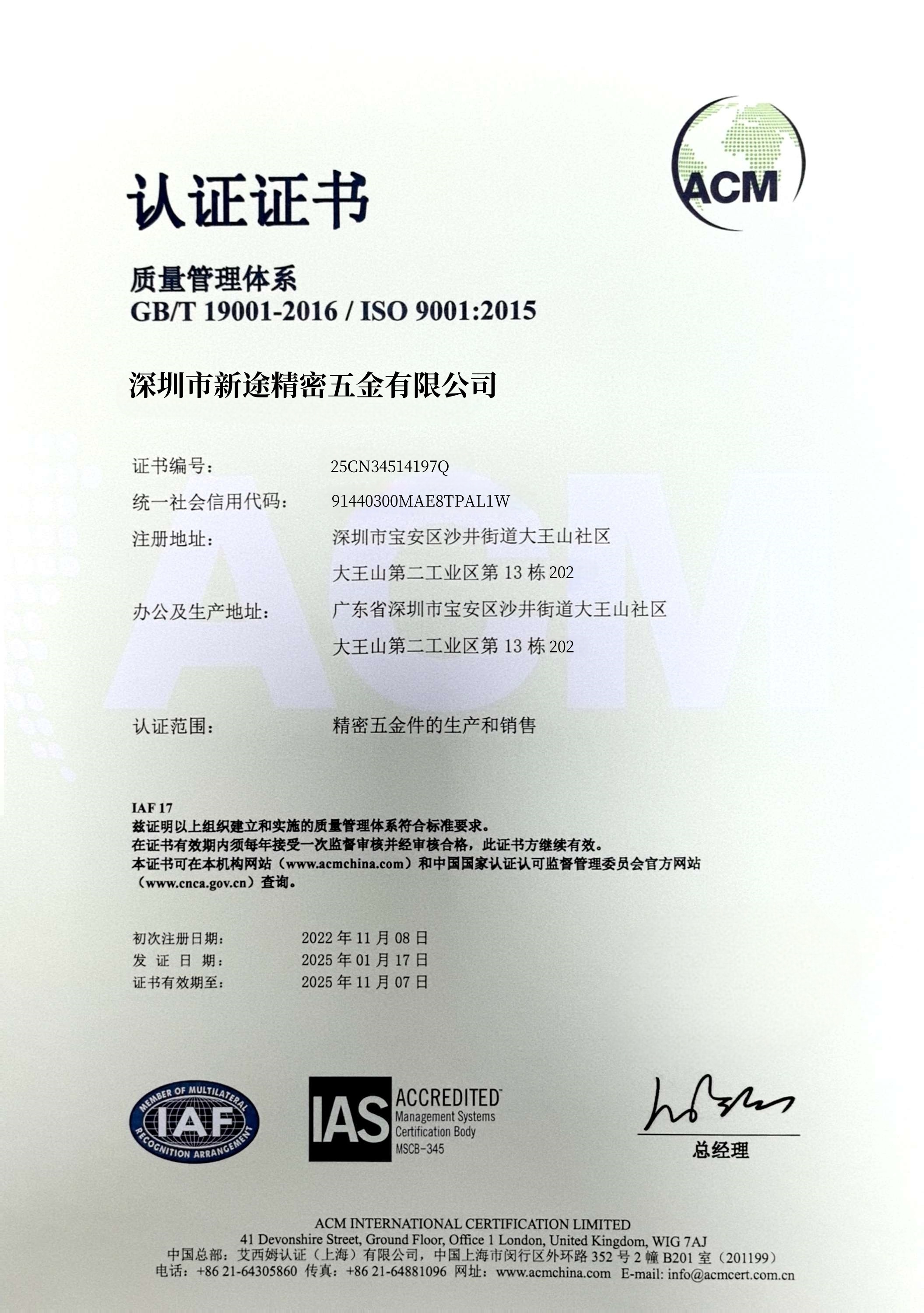
质量认证


Related Products

Shenzhen Nkeyto Precision Hardware Co., Ltd. is a factory specializing in precision hardware processing, committed to providing customers with high-quality products and services.We look forward to working with you.
Contact Us

E-mail: luna@nkeyto.com

Tel: +1 213-221-9094

Add: 13th Building, 202, Dawangshan Second Industrial Zone, Dawangshan Community, Shajing Street, Bao'an District, Shenzhen, Guangdong Province
Powered by: CEglobal
Copryright © 2025 Shenzhen Xintu Precision Hardware Co., Ltd.




Back To Top